Qualcomm says its first HBC chips for the Dragonfly AI250 pass lab tests
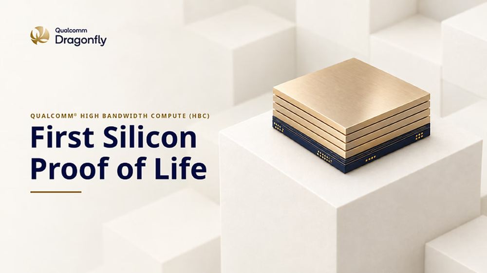
Qualcomm has completed testing the first chips built with its High Bandwidth Compute (HBC) memory technology, clearing a key step towards using it in data centre AI hardware. The company announced the results, saying the technology will feature in its Dragonfly AI250 accelerator, designed to run AI models in data centres. Best known for its […] This story continues at The Next Web
Qualcomm has completed testing the first chips built with its High Bandwidth Compute (HBC) memory technology, clearing a key step towards using it in data centre AI hardware. The company announced the results, saying the technology will feature in its Dragonfly AI250 accelerator, designed to run AI models in data centres.
Best known for its Snapdragon smartphone chips , Qualcomm introduced the Dragonfly brand for its data centre products in June. HBC is designed to address one of the main bottlenecks in running large language models at scale: moving data quickly enough between memory and processors.
The technology places computing capabilities close to memory, reducing the distance data needs to travel. Qualcomm says this increases effective memory bandwidth and improves the amount of work a system can perform per watt.
Testing took place at Qualcomm’s San Diego laboratory using standard automated test equipment. Engineers assessed the full memory read and write path, as well as calculations performed alongside memory. They used random data at sizes representative of commercial products.
Qualcomm said the results confirmed its expected gains in bandwidth and energy efficiency. Comparisons with competing products are estimates adjusted for target operating conditions, however, and actual performance will depend on the final product and workload.
The company has also completed the design of a data centre product using HBC and sent it for manufacturing, a stage known as tape-out. Early bring-up is now underway for a logic chip with layers of DRAM bonded directly on top.
Developing the technology required work with foundry and assembly partners on wafer-to-wafer bonding, which stacks memory directly onto logic chips. The design also includes spare capacity and remapping capabilities, allowing the system to work around defective memory cells.
The project builds on more than a decade of Qualcomm research into stacking memory and logic. The company has previously shipped products with DRAM bonded directly to logic chips and contributed to the development of LPDDR memory standards used in smartphones.
Qualcomm expects the AI250 to begin sampling in the first half of 2027. Its product specifications list 133TB/s of effective memory bandwidth per card, 18 times the figure for its AI200 accelerator.
The card will form part of Dragonfly Rack, Qualcomm’s complete server rack for running AI models. The company is targeting cloud providers, hyperscalers, and large enterprises, positioning the hardware as a way to increase AI computing output while reducing costs and energy consumption.